- 您现在的位置:买卖IC网 > Sheet目录855 > CK2125R68M-T (Taiyo Yuden)INDUCTOR .68UH LAYER 0805
�� �
�
�Precautions� on� the� use� of� Multilayer� chip� inductors�
�Multilayer� chip� inductors� for� high� frequency,� Multilayer� chip� bead� inductors�
�Multilayer� common� mode� choke� coils(MC� series� F� type)�
�■� PRECAUTIONS�
�1.� Circuit� Design�
�◆Verification� of� operating� environment,� electrical� rating� and� performance�
�1.� A� malfunction� in� medical� equipment,� spacecraft,� nuclear� reactors,� etc.� may� cause� serious� harm� to� human� life� or� have� severe� social�
�ramifications.�
�Precautions�
�As� such,� any� inductors� to� be� used� in� such� equipment� may� require� higher� safety� and/or� reliability� considerations� and� should� be� clearly�
�differentiated� from� components� used� in� general� purpose� applications.�
�◆Operating� Current(Verification� of� Rated� current)�
�1.� The� operating� current� for� inductors� must� always� be� lower� than� their� rated� values.�
�2.� Do� not� apply� current� in� excess� of� the� rated� value� because� the� inductance� may� be� reduced� due� to� the� magnetic� saturation� effect.�
�2.� PCB� Design�
�◆Pattern� configurations(Design� of� Land-patterns)�
�1.� When� inductors� are� mounted� on� a� PCB,� the� size� of� land� patterns� and� the� amount� of� solder� used(size� of� fillet)can� directly� affect� inductor�
�performance.�
�Therefore,� the� following� items� must� be� carefully� considered� in� the� design� of� solder� land� patterns:�
�(1)� The� amount� of� solder� applied� can� affect� the� ability� of� chips� to� withstand� mechanical� stresses� which� may� lead� to� breaking� or�
�cracking.� Therefore,� when� designing� land-patterns� it� is� necessary� to� consider� the� appropriate� size� and� configuration� of� the� solder�
�pads� which� in� turn� determines� the� amount� of� solder� necessary� to� form� the� fillets.�
�Precautions�
�(2)� When� more� than� one� part� is� jointly� soldered� onto� the� same� land� or� pad,� the� pad� must� be� designed� so� that� each� component's�
�soldering� point� is� separated� by� solder-resist.�
�(3)� The� larger� size� of� land� patterns� and� amount� of� solder,� the� smaller� Q� value� after� mounting� on� PCB.� It� makes� higher� the� Q� value� to�
�design� land� patterns� smaller� than� terminal� electrode� of� chips.�
�◆Pattern� configurations(Inductor� layout� on� panelized[� breakaway]� PC� boards)�
�1.� After� inductors� have� been� mounted� on� the� boards,� chips� can� be� subjected� to� mechanical� stresses� in� subsequent� manufacturing�
�processes� (PCB� cutting,� board� inspection,� mounting� of� additional� parts,� assembly� into� the� chassis,� wave� soldering� the� reflow� soldered�
�boards� etc.)For� this� reason,� planning� pattern� configurations� and� the� position� of� SMD� inductors� should� be� carefully� performed� to�
�minimize� stress.�
�◆Pattern� configurations(Design� of� Land-patterns)�
�1.� The� following� diagrams� and� tables� show� some� examples� of� recommended� patterns� to� prevent� excessive� solder� amounts(larger� fillets�
�which� extend� above� the� component� end� terminations).� Examples� of� improper� pattern� designs� are� also� shown.�
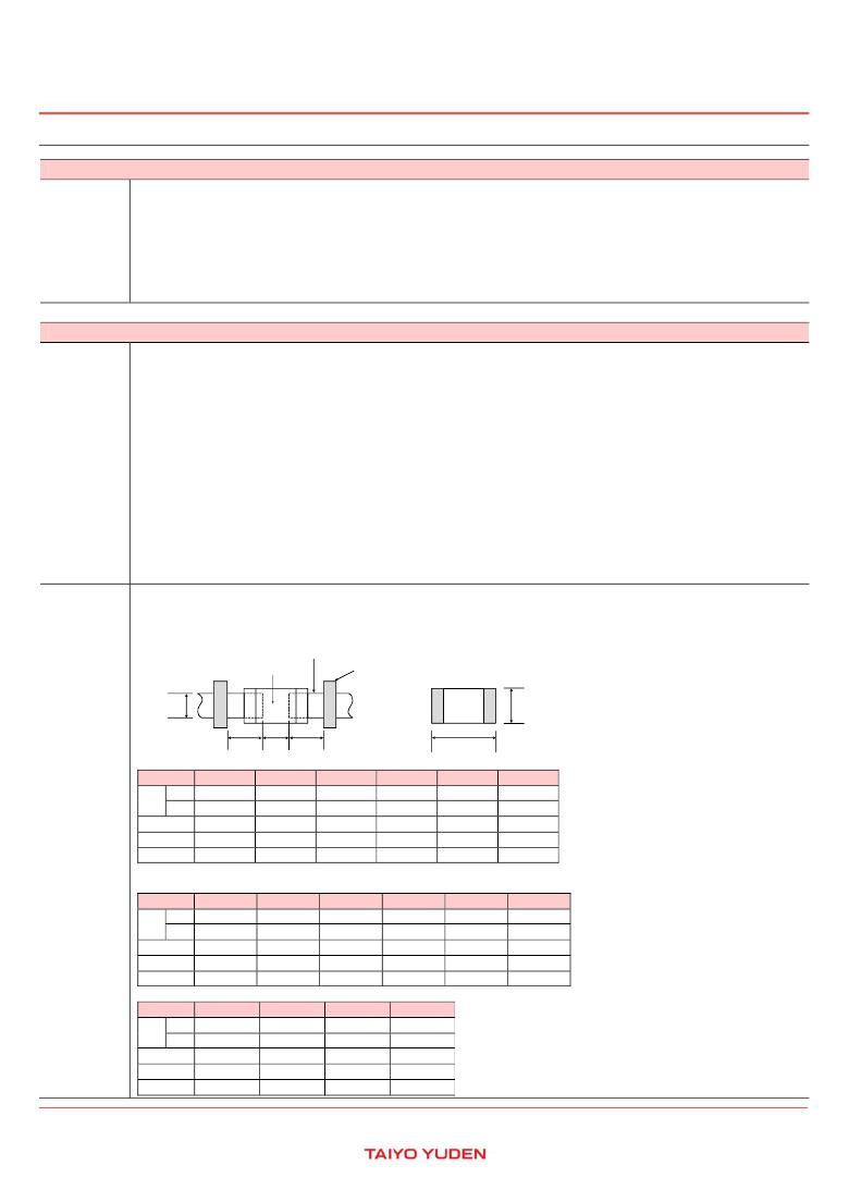
�(1)� Recommended� land� dimensions� for� a� typical� chip� inductor� land� patterns� for� PCBs�
�Land� pattern�
�C�
�Chip� inductor�
�Solder-resist�
�Chip� inductor�
�W�
�B�
�A�
�B�
�L�
�Recommended� land� dimensions� for� wave-soldering�
�(Unit:mm)�
�Type�
�1608�
�2012�
�2125�
�2016�
�2520�
�3216�
�Technical�
�considerations�
�Size�
�L� 1.6� 2.0� 2.0�
�W� 0.8� 1.25� 1.25�
�A� 0.8~1.0� 1.0~1.4� 1.0~1.4�
�B� 0.5~0.8� 0.8~1.5� 0.8~1.5�
�C� 0.6~0.8� 0.9~1.2� 0.9~1.2�
�2.0� 2.5�
�1.6� 2.0�
�1.0~1.4� 1.0~1.4�
�0.8~1.5� 0.6~1.0�
�1.3~1.6� 1.6~2.0�
�3.2�
�1.6�
�1.8~2.5�
�0.8~1.7�
�1.2~1.6�
�Recommended� land� dimensions� for� reflow-soldering�
�(Unit:mm)�
�Type�
�0402�
�0603�
�1005�
�105�
�1608�
�2012�
�Size�
�L� 0.4� 0.6� 1.0�
�W� 0.2� 0.3� 0.5�
�A� 0.15~0.25� 0.20~0.30� 0.45~0.55�
�B� 0.10~0.20� 0.20~0.30� 0.40~0.50�
�C� 0.15~0.30� 0.25~0.40� 0.45~0.55�
�1.0�
�0.6�
�0.50~0.55�
�0.30~0.40�
�0.60~0.70�
�1.6�
�0.8�
�0.8~1.0�
�0.6~0.8�
�0.6~0.8�
�2.0�
�1.25�
�0.8~1.2�
�0.8~1.2�
�0.9~1.6�
�Type�
�2125�
�2016�
�2520�
�3216�
�Size�
�A�
�B�
�C�
�L�
�W�
�2.0�
�1.25�
�0.8~1.2�
�0.8~1.2�
�0.9~1.6�
�2.0�
�1.6�
�0.8~1.2�
�0.8~1.2�
�1.2~2.0�
�2.5�
�2.0�
�1.0~1.4�
�0.6~1.0�
�1.8~2.2�
�3.2�
�1.6�
�1.8~2.5�
�0.6~1.5�
�1.2~2.0�
�?� This� catalog� contains� the� typical� specification� only� due� to� the� limitation� of� space.� When� you� consider� the� purchase� of� our� products,� please� check� our� specification.�
�For� details� of� each� product� (characteristics� graph,� reliability� information,� precautions� for� use,� and� so� on),� see� our� Web� site� (http://www.ty-top.com/)� .�
�i_mlci_prec_e-E02R01�
�发布紧急采购,3分钟左右您将得到回复。
相关PDF资料
CKD31C101H153M
CAP FEEDTHRU 15000PF 50V 1206
CKD710JB0J474S
CAP FEEDTHRU .47UF 6.3V 0402
CKG57NX7S1C107M
CAP CER 100UF 16V 20% X7S 2220
CKP2012N2R2M-T
INDUCTOR 2.2UH MULTILAYER 0805
CLLC1AX7S0G334M
CAP CER 0.33UF 4V 20% X7S 0603
CLS5D11HPNP-100NC
INDUCTOR PWR 1000MA 10UH SMD PB
CM201212-1R0KL
INDUCTOR CHIP 1UH 10% SMD
CM21X5R106K06AL
CAP CER 10UF 4V 10% X5R 0805
相关代理商/技术参数
CK-2125-R68MTK
制造商:KEMET 制造商全称:Kemet Corporation 功能描述:Surface Mount Ferrite Products
CK21KW/MNS
制造商:BM Connecting Cables 功能描述:COTTON GLOVES (MENS)
CK21KW/MNS-20
制造商:BM Connecting Cables 功能描述:LIGHT COTTON GLOVES
CK21M
功能描述:PIPE CLAMP PROBE RoHS:是 类别:测试设备 >> 测试引线 - 热电偶,温度探头 系列:CK 标准包装:1 系列:6543 类型:J 型热电偶 使用:液体,半固体 尖端 - 类型:防浸渍 / 穿透式,圆头 插头类型:超微型(热电偶插头) 探针温度范围:-40 ~ 2000°F(-40 ~ 1093°C) 线缆长度:- 线缆绝缘:- 插头颜色:黑 探针长度:12.000"(304.80mm) 探针材料:-
CK21MC1
功能描述:2 EACH PIPE CLAMP PROBES RoHS:是 类别:测试设备 >> 测试引线 - 热电偶,温度探头 系列:CK 标准包装:1 系列:6543 类型:J 型热电偶 使用:液体,半固体 尖端 - 类型:防浸渍 / 穿透式,圆头 插头类型:超微型(热电偶插头) 探针温度范围:-40 ~ 2000°F(-40 ~ 1093°C) 线缆长度:- 线缆绝缘:- 插头颜色:黑 探针长度:12.000"(304.80mm) 探针材料:-
CK2233
制造商:Lorlin Electronics Ltd 功能描述:
CK2252
制造商:Lorlin Electronics Ltd 功能描述:
CK22803
制造商:Chenbro Micom Usa, Inc. 功能描述:6G 28 PORT SAS EXPANDER CARD, WITH BRACKET - Bulk